 Contact
 Intranet
 SK
SK


Fully 2D physics realized in 3D crystals by breaking their inversion symmetry
Two-dimensional (2D) materials, in general, allow the realization of unique quantum phenomena unattainable in the common three-dimensional (3D) world. A prime example is graphene. Transition metal dichalcogenides (TMDs) have a similar structure. Both can be stacked to form van der Waals heterostructures or can be exfoliated into single layers. But TMDs have an extra variety of excellent properties including strong spin-orbit coupling and superconductivity. In 2D (single atomic layer film) NbSe2, a prominent example of TMD, the combination of these two effects with the crystal symmetries leads to the so-called Ising superconductivity (IS), which can withstand extremely high magnetic fields oriented parallel to the crystal plane. Perhaps more exciting than this resilience against magnetic fields is the potential application of IS in realizing various exotic phenomena such as equal spin Andreev reflections, topological superconductivity, and Majorana fermions.
However, 2D structures are prone to degradation and impractical for applications. 3D materials are robust, easily scalable and accessible to a larger range of scientific analytical techniques. Therefore, it is desirable to find ways of protecting unique features of 2D materials in their 3D counterparts. A common strategy to “embed” 2D behavior into 3D TMDs is to intercalate functional layers between TMD sheets. As evidenced by the growing number of recently published articles, such 3D materials can feature interlayer conductivity, while retaining the properties of 2D TMDs, including IS. While effective, intercalation adds complexity and can introduce extrinsic effects.
A simpler route: symmetry engineering, not chemistry
In their new study, a team from Košice reports that intercalation is not needed. Their study published in Physical Review Letters demonstrates, how an even more straightforward approach leads to analogous results. Just breaking the inversion symmetry of the otherwise centrosymmetric crystal lattice without any intercalation is sufficient to protect IS in bulk NbSe2. Unlike the most common 2H-NbSe2, the 4Ha-NbSe2 polytype prepared at higher temperatures, with four NbSe2 atomic layers stacked as shown in the figure, has broken symmetry.
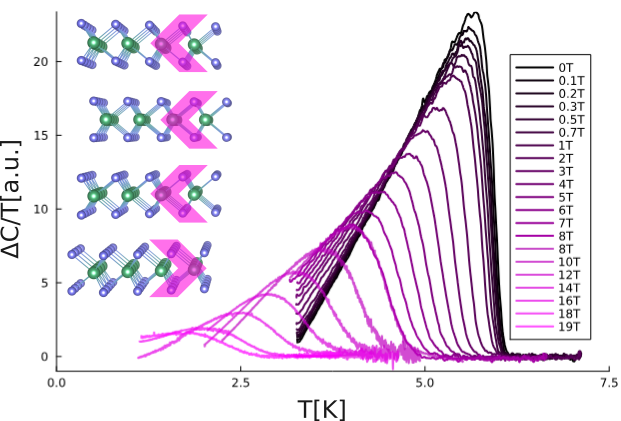
Since the difference between the two polytypes is subtle, the authors first used various experimental techniques to unambiguously determine the crystal structure of the sample. Then, they employed heat capacity measurements to demonstrate, that bulk superconductivity in 4Ha-NbSe2 single crystal withstands magnetic fields almost three times the Pauli limit. Heat capacity measurements characterize the bulk properties of the sample; therefore, they are superior to the transport measurements employed in former studies, which can suffer from other spurious 2D effects not characteristic of the bulk. Finally, utilizing the obtained crystallographic parameters, they ab initio calculated the band structure of the 4Ha-NbSe2 polytype and justified the presence of IS.
Why it matters
The findings show that stacking order and symmetry – not just chemical composition – can be used to tune fundamental electronic properties in bulk TMDs. This symmetry‑only approach streamlines materials design, avoids chemical complexity, and offers a robust, scalable platform for exploring and exploiting Ising superconductivity in realistic devices. It opens new pathways.
Figure:
Heat capacity of 4Ha-NbSe₂ measured up to 19 T. Inset: Crystal structure of 4Ha-NbSe₂, where unit cell is from 4 layers.
DOI: https://doi.org/10.1103/qxb4-sf28